

ASML’s fifth High-NA system shipment measured ecosystem progress, not HVM
ASML said it shipped its fifth High-NA EUV system in Q1 2025 and had systems at three customers. Shipment counts are readiness signals, not proof of high-volume chip output.
Historical reporting: ASML’s April 16, 2025 results said it shipped its fifth High-NA system in Q1 and had systems at three customers. The EXE:5000 product page describes the platform; analysis below is editorial.
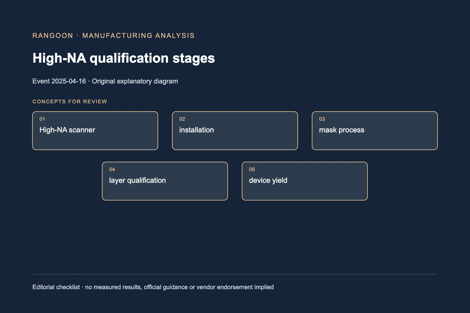
Key takeaways
- ASML reported a fifth High-NA shipment and installations at three customers in Q1 2025.
- A scanner shipment does not prove a customer’s high-volume product output.
- Tool readiness, process qualification, mask ecosystem, and device yield are separate conditions.
What ASML reported[source 1][source 2]
On April 16, 2025, ASML reported that it had shipped its fifth High-NA system in the first quarter and that the systems were at three customers. This was a concrete ecosystem-progress milestone: more than one customer had access to the new lithography platform for installation and development work.
ASML describes its TWINSCAN EXE:5000 as the first 0.55 numerical-aperture, or High-NA, EUV system and explains its resolution and imaging differences from NXE systems. The product description explains capability goals. It does not establish that a receiving fab has qualified every layer, mask, resist, overlay target, and yield requirement needed for high-volume device manufacturing.
Editorial analysis: a tool shipment is not a chip-output metric
A lithography tool can arrive before a fab has completed installation, process matching, resist selection, mask preparation, overlay tuning, defect learning, and device integration. Each step is needed before a tool’s optical potential appears as dependable product yield. Treating a shipment count as chip capacity skips the work that turns equipment into a stable manufacturing flow.
A readiness map can list tool acceptance, installation, source performance, process window, mask infrastructure, resist qualification, layer qualification, device yield, and product release. Each item has different owners and evidence. The map is more useful than an aggregate claim that High-NA is ‘ready’ without saying ready for which task.
Editorial analysis: High-NA changes several interfaces
High-NA EUV affects optics, exposure field, masks, resists, computational lithography, metrology, and device design rules. A customer may be advanced in one part of that ecosystem while still learning another. This is why public tool milestones should be read as input to a qualification program, not as a substitute for the program’s results.
For each target layer, a manufacturer can retain exposure recipe, mask revision, resist lot, defect inspection method, overlay result, electrical test outcome, and yield evidence. That evidence can show where a performance benefit is real and where a production constraint persists.
Editorial analysis: define readiness before counting it
A project dashboard should define whether readiness means tool delivery, tool acceptance, process demonstration, qualified device layer, pilot production, or volume product. These names should be stable across suppliers, so a hardware planner can compare dependencies without converting every positive update into the same green status.
ASML’s April 2025 update is significant because it gave a count and customer footprint. Its bounded meaning is equally important: it documented platform distribution, not the completion of every downstream manufacturing gate.
Editorial analysis: separate field learning from capacity
Systems installed at several customers can accelerate field learning through different layouts, resists, metrology, and integration approaches. That ecosystem fact matters even when no capacity figure is public. Record the specific learning objective and result for each customer program rather than inferring that a scanner fleet has reached uniform process maturity. Compare results only when process conditions and target layers are sufficiently aligned to make the comparison meaningful. Otherwise record the difference as a constraint on inference.
Sources
- ASML: Q1 2025 financial results (April 16, 2025)
- ASML: TWINSCAN EXE:5000
Continue reading
Related reading
 News analysisASML’s EXE:5200B shipment showed High-NA progress still needed process proof3 min read
 News analysisNVIDIA’s memory codesign post highlights a practical boundary between capacity and usable agent throughput3 min read
 News analysisNVIDIA supply-chain capacity plans make packaging, test and optics explicit infrastructure constraints3 min read