

Lam introduced VECTOR TEOS 3D for inter-die gapfill in advanced chip packaging
Lam introduced VECTOR TEOS 3D on September 9, 2025 as a deposition tool for inter-die gapfill in 3D chip stacking and heterogeneous packaging for AI and HPC.
Historical reporting: Lam announced VECTOR TEOS 3D on September 9, 2025 as an advanced-packaging deposition tool. A Lam packaging explainer supplies the chiplet and packaging context. The sources establish a named equipment release and Lam’s stated installation claim; they do not establish a particular package yield, customer qualification, production volume, or an AI-system performance result.
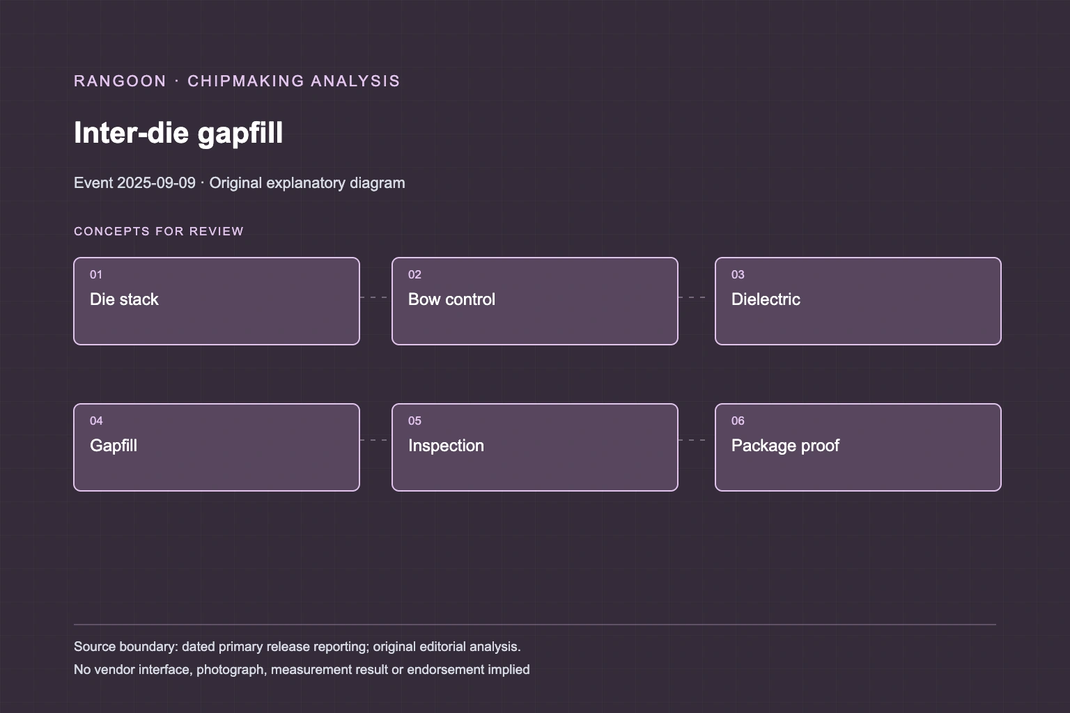
Key takeaways
- VECTOR TEOS 3D was announced for inter-die gapfill in advanced packaging.
- Lam positioned it around bowed wafers and 3D integration process challenges.
- Installation at leading fabs does not identify customers, qualification status or output volume.
The September announcement targeted a packaging process step, not a finished chip product[source 1][source 2]
Lam introduced VECTOR TEOS 3D on September 9, 2025 as a deposition tool for advanced packaging. The company described ultra-thick inter-die gapfill for 3D stacking and high-density heterogeneous integration, applications relevant to AI and high-performance computing packages. This is a manufacturing-equipment event. It concerns a process used to place and protect multiple dies in a package, not the release of a GPU, a memory stack or a new chiplet interconnect standard. Lam’s announcement identifies the process problem it intends to address, including stressed and bowed wafers. It does not disclose the full package flow used by any customer, the product mix on a line, or a package’s final electrical or thermal performance.
Gapfill and wafer handling are stated process features, not a public package recipe[source 1]
The launch describes a bowed-wafer handling approach, dielectric deposition and monitoring through Lam Equipment Intelligence. Those are meaningful statements about the tool’s proposed process role. They do not disclose thickness targets for every customer, deposition chemistry, thermal budget, die geometry or the sequence of bonding, underfill, inspection and test that produces a sellable package. Advanced packaging joins multiple parts whose interfaces must be qualified together. A uniform film result in one application cannot be assumed to settle warpage, reliability or yield in another. The archive keeps the technical description at the level Lam published: a tool intended to improve inter-die gapfill and process repeatability. It avoids inventing a chip-package architecture or asserting a production recipe that the sources do not provide.
Lam’s installation statement is not the same as disclosure of customer production status[source 1]
Lam says VECTOR TEOS 3D is installed at leading logic and memory fabs around the world. That statement is stronger than an unreleased concept, yet it does not name the fabs, say whether each installation has completed qualification, or give a date and volume for production output. “Installed” can cover different stages, including evaluation, process development and production preparation. The source also does not state how many systems were placed, what package generation they support, or whether customers achieved a target yield. Packaging equipment may be deployed before an end product is broadly available. The historical event can therefore record Lam’s stated installed-base status while separating it from customer adoption, high-volume manufacturing and the performance of any downstream AI system.
Equipment availability needs separate proof from package and AI-workload outcomes[source 1][source 2]
The news value lies in a named tool aimed at a difficult advanced-packaging process. Neither Lam source reports a customer’s completed package qualification, measured defect-rate change or AI-workload throughput. Nor do they establish that a tool feature automatically reduces package cost or energy use across diverse stacks. These outcomes depend on die design, substrates, bonding, testing and system integration as well as deposition. The archive records Lam’s release, intended use and public installation statement. It does not turn equipment marketing language into a universal manufacturing or workload result. Later customer disclosures could show a specific qualification or production ramp, but they would be distinct events with their own dates and evidence.
Sources
- Lam Research: VECTOR TEOS 3D advanced-packaging announcement (September 9, 2025)
- Lam Research: The AI Revolution Relies on Advanced Packaging (September 18, 2025)
Continue reading
Related reading
 News analysisLam introduced Fabtex Yield Optimizer for high-volume fab process variability work3 min read
 News analysisApplied Materials introduced Kinex, Xtera and PROVision 10 for logic, memory and packaging process work3 min read
 News analysisApplied unveiled the EPIC Center as a collaborative chipmaking R&D facility, with HVM still a future transfer step3 min read