

Applied unveiled the EPIC Center as a collaborative chipmaking R&D facility, with HVM still a future transfer step
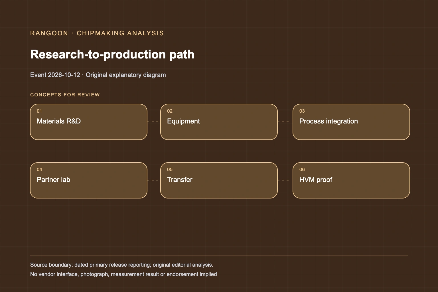
Applied Materials unveiled its EPIC Center on October 12, 2026, a $5 billion collaborative semiconductor R&D facility intended to move innovations toward high-volume manufacturing.
Historical reporting: Applied Materials unveiled the EPIC Center on October 12, 2026 and described a $5 billion collaborative R&D facility for semiconductor process and equipment work. Applied’s event and media records identify the launch and supporting materials. The sources establish an R&D-facility unveiling and participant roster; they do not establish a completed production line, transferred customer process, high-volume output or measured AI-chip result.
Key takeaways
- Applied unveiled EPIC as collaborative semiconductor process and equipment R&D infrastructure.
- The company framed the centre as a path from research toward high-volume manufacturing.
- An R&D-facility unveiling is not evidence of a transferred customer process or chip output.
EPIC opened as an R&D and commercialization facility, not a finished customer fab[source 1][source 2]
Applied Materials unveiled its Equipment and Process Innovation and Commercialization Center on October 12, 2026. The company described a $5 billion capital investment in a collaborative facility for semiconductor process technology and manufacturing-equipment research and development. The announcement matters because it frames a physical place for materials researchers, equipment builders, chipmakers and universities to work together. It does not announce a new foundry producing customer wafers or a line already shipping AI chips. Applied presents EPIC as a way to shorten the path from breakthrough research toward high-volume manufacturing. A path toward HVM is not the same evidence state as HVM output, and the release does not claim that a customer process had already been transferred from EPIC into a production fab.
The roster identifies collaborators without proving a shared production programme[source 1]
Applied lists founding, innovation and research participants from chipmakers, systems companies, equipment partners and universities. A participant roster supports the claim that the centre had a collaborative structure at unveiling. It does not disclose the terms of each project, which partners would use which tools, or whether every listed organisation had committed the same resources. The sources also do not identify a jointly qualified device or an output schedule. Collaboration can include research, process development, evaluation and workforce work before any technology reaches a customer fab. The archive records the public roster and the stated co-innovation purpose. It does not infer a particular product relationship, process transfer or high-volume manufacturing result for a named partner.
A facility built to accelerate commercialization still needs separate execution evidence[source 1][source 2]
Applied’s description of EPIC emphasises reducing handoffs between materials research, equipment and process integration. That is a business and operating model claim. Its achievement depends on future projects, technical results, customer qualification and manufacturing transfer. The sources do not present cycle-time measurements, a public baseline for prior handoffs or independent evidence that a specific project reached production faster. They also do not establish that every research outcome is suitable for a commercial node. This boundary is central to the news: EPIC was unveiled as infrastructure intended to change how semiconductor innovations move toward production. The archive preserves that intent while separating it from actual product qualification, customer adoption and high-volume manufacturing, which require later records.
The unveiling does not provide a chip-output, yield or AI-performance scorecard[source 1][source 2]
The EPIC event establishes a facility launch, disclosed capital scale and Applied’s stated strategy for collaborative process innovation. It does not disclose wafer starts, customer yield, installed tool counts, chip shipments or a measured AI-workload result. No source provides an independent audit of facility utilisation or a completed transfer to a named foundry. Those omissions are expected at an R&D-infrastructure event, but they limit what historical reporting can claim. The archive therefore treats October 12 as the date of an R&D-facility unveiling. Future reporting can document the first transferred process, production use or output result if a primary source gives a specific technology, time and measurement.
Sources
- Applied Materials: Unveils $5 billion EPIC Center (October 12, 2026)
- Applied Materials: EPIC Center unveiling event (October 12, 2026)
Continue reading
Related reading
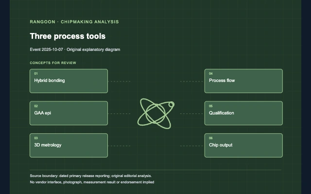 News analysisApplied Materials introduced Kinex, Xtera and PROVision 10 for logic, memory and packaging process work3 min read
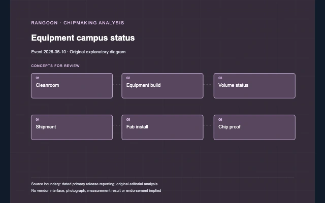 News analysisApplied disclosed Singapore equipment manufacturing already at volume production, while the public release date remained distinct3 min read
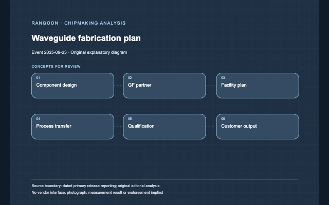 News analysisApplied and GlobalFoundries announced a Singapore waveguide fabrication collaboration for AI-era photonics3 min read