

Applied Materials introduced Kinex, Xtera and PROVision 10 for logic, memory and packaging process work
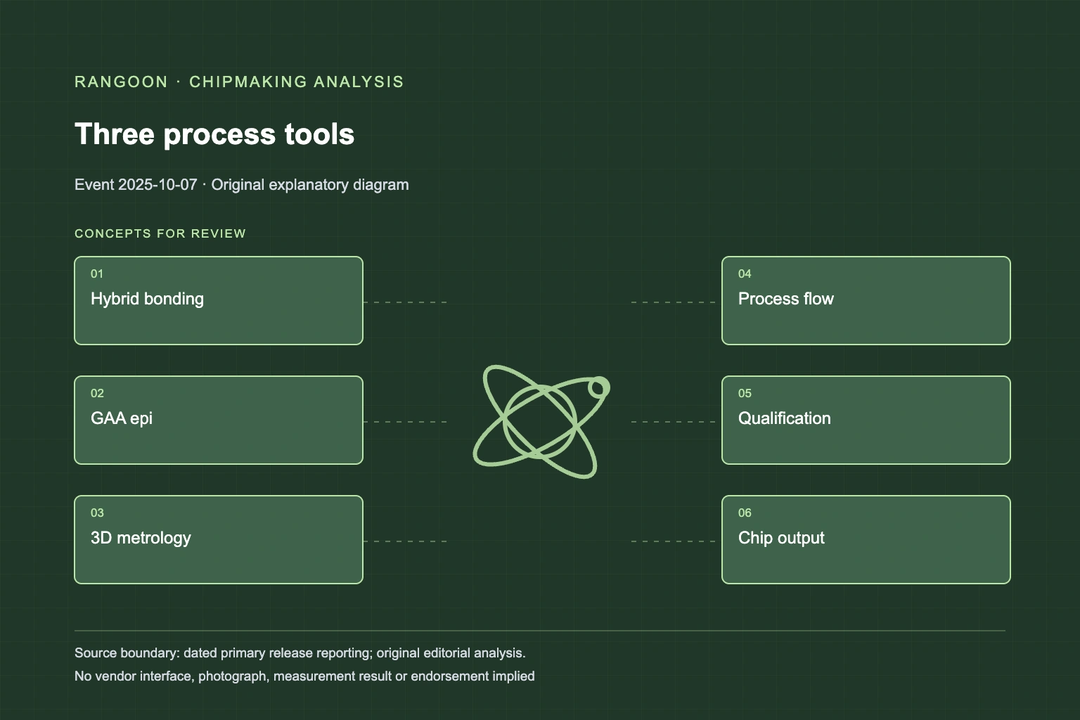
Applied Materials introduced Kinex, Xtera and PROVision 10 on October 7, 2025, targeting hybrid bonding, gate-all-around epitaxy and 3D-chip metrology.
Historical reporting: Applied Materials announced Kinex, Xtera and PROVision 10 on October 7, 2025. Its media-kit record supplies product-family context. The sources establish three equipment introductions and their stated target process areas; they do not establish customer qualification, high-volume output, independent yield results or a single integrated manufacturing flow using all three systems.
Key takeaways
- Applied announced separate systems for hybrid bonding, GAA epitaxy and e-beam metrology.
- The products target different stages of logic, memory and package manufacture.
- A product launch does not establish customer qualification or measured device performance.
Applied announced three systems with separate manufacturing roles[source 1][source 2]
On October 7, 2025, Applied Materials introduced Kinex, Xtera and PROVision 10 as chipmaking systems for AI-era logic, memory and advanced packaging. Kinex was presented as an integrated die-to-wafer hybrid-bonding system; Xtera as an epitaxy system for gate-all-around transistors; PROVision 10 as e-beam metrology for complex 3D chips. Grouping them in one announcement does not make them one machine or one production process. Each addresses a different manufacturing stage and must be evaluated within an individual process flow. The release establishes that Applied publicly launched the equipment family and stated its target applications. It does not identify which customers bought the systems, whether they were accepted on a production line or how a particular chip maker combined them.
Hybrid bonding is a packaging process claim that needs device-level proof separately[source 1]
Applied describes Kinex as an integrated die-to-wafer hybrid-bonding system. Hybrid bonding is a way to join dies directly, but an equipment announcement does not disclose a customer’s bond pitch, die stack, reliability qualification or package yield. The source frames the system as enabling lower-power and higher-performance logic and memory chips. That is the company’s expected application outcome, not a published test result for a named device. Packaging performance depends on interfaces across dies, materials, thermal management, test and system design. The archive can accurately say that Kinex was introduced for a specific packaging process. It cannot claim that a released tool itself delivered a measured package advantage without later customer or independent evidence tied to a particular configuration.
The logic and metrology products address different constraints from package bonding[source 1][source 2]
Xtera targets void-free epitaxial layers for gate-all-around transistor work at 2nm and beyond, while PROVision 10 targets inspection and measurement of complex 3D structures. These descriptions show why Applied packaged the launches together: AI hardware demands progress in transistor formation, memory and packaging. But the systems do not prove one another’s results. A metrology resolution specification does not establish device yield; an epitaxy claim does not establish a completed node qualification; a hybrid-bonding product does not establish full-chip power. The sources do not provide a full performance comparison, a process-control plan or an independent benchmark across tools. Historical reporting should retain the product distinctions so a later manufacturing result is not retroactively assigned to every system in the October announcement.
Equipment introductions are upstream events, separate from high-volume chip output[source 1][source 2]
Applied’s October launch marks an upstream manufacturing capability announcement. The company said the products can help customers build future AI chips, but neither source reports high-volume chip output, a shipped package, customer yield data or an independently verified performance-per-watt result. The materials also do not disclose a common qualification schedule or indicate that every tool was equally mature on the announcement date. Semiconductor equipment can be released, installed, evaluated and qualified over different timelines. The archive records the named systems and their stated process roles. Any claim about a commercial chip, mass production, reliability or AI-system benefit requires its own later evidence from a specific device and manufacturing programme.
Sources
Continue reading
Related reading
 News analysisLam introduced VECTOR TEOS 3D for inter-die gapfill in advanced chip packaging3 min read
 News analysisApplied unveiled the EPIC Center as a collaborative chipmaking R&D facility, with HVM still a future transfer step3 min read
 News analysisApplied disclosed Singapore equipment manufacturing already at volume production, while the public release date remained distinct3 min read