

SK hynix said its HBM4 development was complete and its mass-production system was ready
SK hynix announced on September 12, 2025 that it had completed HBM4 development and readied a mass-production system after March samples.
Historical reporting: SK hynix announced on September 12, 2025 that it had completed HBM4 development and prepared a mass-production system. Its March 2025 sample shipment was an earlier qualification event, not the same event. Bandwidth, power-efficiency, operating-speed, and service-performance statements are SK hynix claims; this article does not claim volume shipments, customer qualification, or measured system results.
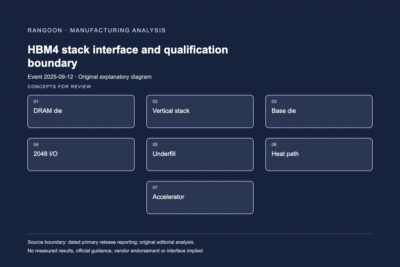
Key takeaways
- The September event was development completion and production-system readiness, distinct from both March samples and demonstrated customer supply.
- HBM4’s 2,048 I/O count changes interface bandwidth, while stacked-memory packaging still shapes power and thermal limits.
- Vendor performance projections should remain separate from customer qualification and full-system measurement.
The September record was readiness for mass production, not a generic HBM4 launch[source 1]
SK hynix announced on September 12, 2025 that it had completed HBM4 development and prepared a mass-production system. The company said the product used 2,048 I/O terminals, twice the count it cited for the preceding generation, and described more than 10Gbps operating speed. It also said it was ready to supply customers according to their plans.
Those statements establish a vendor-reported manufacturing-readiness milestone. They do not establish that every customer had qualified the memory, that a particular accelerator shipped with it, or that system volume deliveries had occurred on that date.
March samples and September production readiness answered different questions[source 1][source 2]
In March 2025, SK hynix reported shipping 12-layer HBM4 samples to customers and said certification work would follow. That earlier event concerned evaluation material and a path toward preparation, while the September announcement described completed development and an established mass-production system. Keeping the two dates separate prevents a sample from being counted as production supply or a readiness statement from being rewritten as a customer deployment.
The difference matters because stacked-memory qualification crosses memory behavior, base-die logic, package warpage, thermal response, and the host accelerator interface. A customer can need its own validation cycle after a memory supplier has finished development.
More interface lanes do not eliminate the package constraints of stacked memory[source 1]
HBM increases data movement by vertically stacking DRAM dies and connecting the stack through a wide interface rather than relying on a conventional narrow external memory bus. SK hynix attributed HBM4 bandwidth gains to the doubled I/O count and said it used an advanced MR-MUF process and a 1bnm DRAM process. The company described MR-MUF as a way to manage warpage and heat dissipation in the stack.
Those engineering choices expose tradeoffs rather than a free performance gain. Higher transfer capability still has to coexist with package yield, signal integrity, cooling, power delivery, controller behavior, and an accelerator’s ability to consume the bandwidth.
Vendor bandwidth and efficiency figures are inputs to validation, not deployment proof[source 1][source 2]
SK hynix said its HBM4 bandwidth doubled and power efficiency improved by more than 40 percent compared with the prior generation, and projected an AI-service performance improvement when applied. Those are supplier-reported comparisons with unstated system configurations in the launch material. They cannot establish a result for a different stack height, accelerator, workload, cooling design, or memory-access pattern.
A system evaluation needs to identify the memory revision, accelerator firmware, model workload, batch size, precision, power cap, and thermal condition. Without that context, a bandwidth figure may describe a useful component property but not the bottleneck that decides application throughput. Bandwidth-bound inference makes that dependency especially visible.
Sources
Continue reading
Related reading
 News analysisSamsung said it began HBM4 mass production and commercial shipment3 min read
 News analysisSK hynix’s HBM4 samples marked a qualification stage, not volume supply3 min read
 News analysisNVIDIA supply-chain capacity plans make packaging, test and optics explicit infrastructure constraints3 min read