

Applied and GlobalFoundries announced a Singapore waveguide fabrication collaboration for AI-era photonics
Applied Materials and GlobalFoundries announced a September 23, 2025 waveguide-fabrication facility plan for Singapore, naming GF as high-volume manufacturing partner.
Historical reporting: Applied Materials announced on September 23, 2025 a collaboration with GlobalFoundries to establish a waveguide fabrication facility at GF Singapore, and named GF as the high-volume manufacturing partner. Applied’s later media materials describe the waveguide manufacturing context. The sources establish a partnership and stated manufacturing role; they do not establish a completed facility, commercial output, customer qualification, or a deployed AI-photonics product.
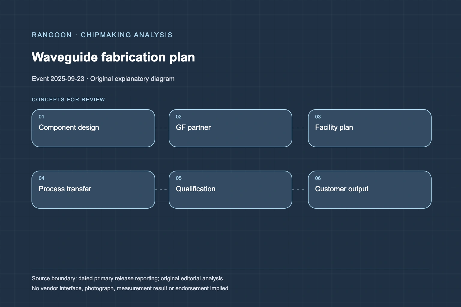
Key takeaways
- Applied and GF announced a Singapore waveguide fabrication collaboration.
- GF was named as the intended high-volume manufacturing partner.
- A facility plan does not establish completed output, qualification or AI-system deployment.
The partnership announced a waveguide-fabrication path rather than a finished photonics product[source 1][source 2]
Applied Materials and GlobalFoundries announced on September 23, 2025 that they would establish a waveguide fabrication facility at GF Singapore. Applied said it would develop waveguide components and named GF as the high-volume manufacturing partner. The event concerns a manufacturing collaboration for photonic components, which the companies linked to emerging AI and augmented-reality applications. It does not announce a completed optical module, a shipped AI system or a production record from a finished facility. Manufacturing partnerships commonly begin before a line reaches customer qualification and volume output. The source does not identify a first customer, disclose a capacity figure, name a process node or set a public timeline for commercial shipments.
Development and high-volume manufacturing are separate roles in the disclosed plan[source 1]
The release assigns Applied a component-development role and GlobalFoundries a high-volume manufacturing role. That distinction is useful because it avoids treating a materials or process developer as the operator of every later factory step. It also does not establish that the roles had already delivered qualified parts on the announcement date. Waveguide fabrication can involve materials, patterning, packaging, optical testing and integration decisions that are not fully described in the public release. The sources do not publish process recipes, manufacturing yield, inspection criteria or reliability data. The archive therefore records the announced division of work and leaves the physical output boundary clear: a named manufacturing partner is evidence of an intended production path, not proof that a high-volume product had been made.
AI and AR application language describes a target market, not a performance result[source 1][source 2]
Applied linked the collaboration to an AI-driven photonics inflection and to waveguides for augmented-reality glasses. Such applications require optical components, but the announcement does not show that a particular headset or data-centre system used the planned output. It also does not provide a link budget, optical loss measurement, device power result or end-user performance comparison. A waveguide component can be an important manufacturing input without determining the complete behavior of a system. The sources supply no independent benchmark against another waveguide technology and no public qualification record. The historical story is therefore about a disclosed fabrication collaboration and its stated markets, not a claim that the collaboration had delivered an AI-product advantage at launch.
A collaboration announcement requires later factory and customer records to show execution[source 1][source 2]
The September sources establish that Applied and GF publicly stated their plan and roles. They do not establish construction completion, tool installation, qualified process capability, production volume or a contract for customer deliveries. Nor do they establish a measured AI-infrastructure benefit. These distinctions matter because the journey from a materials process to a commercial photonics component includes technical transfer, manufacturing readiness and customer testing. The archive records the initial collaboration without importing later milestones that the sources do not document. Future evidence can show a facility opening, a qualification or a product shipment, each as a separate event with its own date and measurement basis.
Sources
Continue reading
Related reading
 News analysisApplied unveiled the EPIC Center as a collaborative chipmaking R&D facility, with HVM still a future transfer step3 min read
 News analysisApplied Materials introduced Kinex, Xtera and PROVision 10 for logic, memory and packaging process work3 min read
 News analysisApplied disclosed Singapore equipment manufacturing already at volume production, while the public release date remained distinct3 min read