

NVIDIA introduced NVLink Fusion for semi-custom AI infrastructure
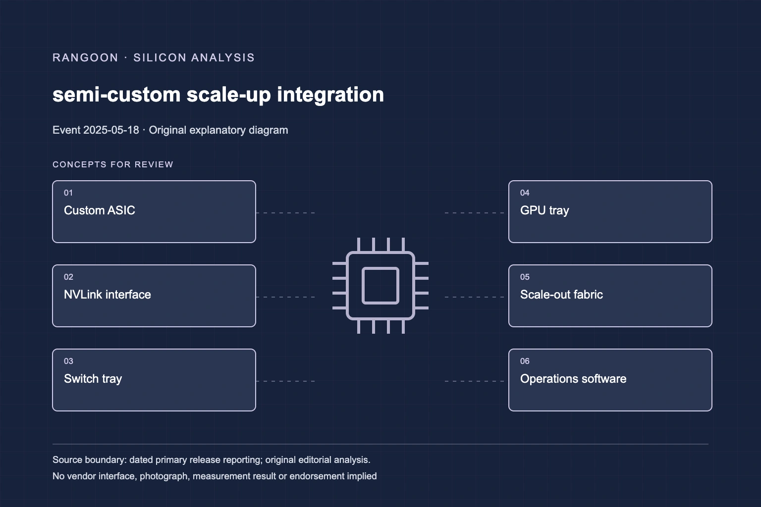
NVIDIA introduced NVLink Fusion on May 18, 2025, describing a route for partner ASICs and CPUs to join an NVLink-based rack-scale AI infrastructure design.
Historical reporting: NVIDIA's May 18 press release establishes the NVLink Fusion announcement. Its same-day technical blog was freshly read for architecture context. Partner plans and NVIDIA bandwidth or performance figures are supplier statements, not evidence of a delivered customer system.
Key takeaways
- NVLink Fusion was an announced semi-custom scale-up option, not proof that a partner system had deployed.
- NVIDIA described partners connecting custom CPUs or ASICs with its rack, fabric and operations components.
- A heterogeneous rack needs product-specific electrical, software, cooling and service validation.
NVIDIA announced a partner path into its scale-up fabric[source 1][source 2]
At COMPUTEX on May 18, 2025, NVIDIA introduced NVLink Fusion as silicon intended to let partners build semi-custom AI infrastructure with its NVLink ecosystem. The press release names MediaTek, Marvell, Alchip, Astera Labs, Synopsys and Cadence as early adopters, and says Fujitsu and Qualcomm planned custom CPUs coupled with NVIDIA GPUs. This records an announced integration direction. It does not establish that one of those planned systems was available, qualified or running a customer workload on that date.
The technical material places the link inside a larger rack design[source 1][source 2]
NVIDIA's technical post describes NVLink Fusion alongside NVLink Switch chips, Grace CPUs, ConnectX SuperNICs, BlueField DPUs, Quantum and Spectrum-X switches, and Mission Control. It says an NVLink Switch chip can provide 130 TB/s of GPU bandwidth in a 72-GPU NVLink domain. These are NVIDIA architectural and performance statements. The list matters because semi-custom silicon is only one part of a rack: it must meet fabric, I/O, management, power and cooling constraints. A custom device connected to a common fabric is not automatically interchangeable with every GPU or CPU configuration.
Adopter language and product delivery are separate evidence categories[source 1][source 2]
The release uses adoption and planned-build language for its listed ecosystem members. That is useful supplier-roadmap evidence, but it is not a shipping-system receipt. A later product would need its own information about supported custom silicon, physical interface, firmware, topology, availability and operating software. Likewise, a stated rack-level performance relationship cannot be assigned to a future partner device without a controlled comparison. Heterogeneous systems need end-to-end checks for memory semantics, collective communication, error recovery and scheduler behavior, especially when their compute elements differ.
NVLink Fusion changed the partner-integration surface, not the status of partner systems[source 1][source 2]
NVIDIA's release identifies a set of early adopters and separately says Fujitsu and Qualcomm planned custom CPUs coupled with NVIDIA GPUs. Those verbs matter: the May record announced an ecosystem and a route for semi-custom compute, rather than reporting shipments from each named partner. NVIDIA's technical post places the route alongside NVLink Switch chips, Grace CPUs, ConnectX SuperNICs, BlueField DPUs, Quantum and Spectrum-X switches, and Mission Control. It also describes a 72-GPU NVLink domain and a claimed 130 TB/s of GPU bandwidth. The press release adds up to 800 Gb/s throughput through ConnectX-8 SuperNICs, Spectrum-X Ethernet and Quantum-X800 InfiniBand, with co-packaged optics described as coming soon. It lists AIchip, Fujitsu, MediaTek, Marvell and Qualcomm among early adopters. It frames those components as scale-out alongside any ASIC and rack-scale systems. These are NVIDIA architectural statements showing the surrounding rack layers; they do not become a measured result for a future custom ASIC or CPU.
Sources
- NVIDIA: NVLink Fusion announcement (May 18, 2025)
- NVIDIA Technical Blog: NVLink Fusion rack-scale architecture (May 18, 2025)
Continue reading
Related reading
 News analysisNVIDIA’s memory codesign post highlights a practical boundary between capacity and usable agent throughput3 min read
 News analysisNVIDIA supply-chain capacity plans make packaging, test and optics explicit infrastructure constraints3 min read
 News analysisPCI-SIG released PCIe 7.0 to members at 128 GT/s3 min read